SeeedFusion PCB Service

Seeed were kind enough to offer me a coupon towards their Seeed-Fusion PCB service. I had a design ready which I had recently converted from Eagle to KiCad so it seemed like an excellent opportunity to try them out.

Board pricing structure

I am a maker, building things in my spare time, so I tend to make small boards in low quantities. The SeeedFusion pricing structure is optimized for larger boards at larger volumes. However, they usually have a offer in place to encourage prototypers and makers  to use their service for smaller volumes. When I ordered the offer was $9.90 for 10 boards up to 100mm by 100mm, at the time of writing the price has been reduced to $4.90.

This is an excellent deal if you want ten 100mm by 100mm boards, but it isn’t great if you just want a few small boards. 100mm by 100mm is larger than a Raspberry Pi or an Arduino. The board I had in mind was 0.8″ by 0.5″ (20.32mm x 12.7mm). The result of the special offer is that introduces a discontinuity in the pricing structure. I made the chart below to illustrate how the pricing in US dollars per square inch changes with board size and quantity by plugging different parameters into the order form.

In my case ten boards would have cost $9.90 whereas 30 boards cost $11.78 so I decided I might as well go for 30 boards.

Shipping costs

Free shipping is a wonderful thing because you don’t have to factor shipping costs into your purchase decision. However SeeedFusion charges shipping even on small orders. When I order components from AliExpress I usually get free or less than $2 China Post ePacket shipping to the US for small items. It would be great if SeeedFusion could offer a similar service on small orders.

The cheapest shipping option on my one ounce order was $11.52. So even at 30 boards this doubles the price of the board. In my case this added up to $0.78 per board.

I expect the shipping costs increase as the order size increases, but you don’t get to see the shipping cost until you add an order to your cart. So making the overly simplistic assumption that shipping on all order sizes is $11.52 we get the following price chart.

Stencils

Seeed-Fusion stencils start at $19.90 which is a reasonable price. However when I added a stencil to my cart it added $32.85 to my shipping costs. The reason is that the smallest stencil is 28cm by 38cm which is larger than a letter size sheet of paper. I like using a stencil for SMD boards, but I want a nice small stencil for prototyping as I am only making one board at a time.

HASL or ENIG finish

Exposed copper pads tarnish quickly, so they need to be finished to protect them. The prices above are for HASL which is basically a layer of solder on the exposed copper. Another option is ENIG which is an electroless nickel plating covered with a thin layer of immersion gold.

ENIG is flatter than HASL and doesn’t migrate during reflow so it is a better choice for fine pitched SMD parts and strongly recommended for BGAs.

The prices above jump dramatically (e.g. from $9.90 to $29.90 for 10 boards) when you check the box for ENIG. For my board with 0603 SMD components and 0.5mm pitch IC leads HASL is fine.

DRC Rules

When ordering from a PCB fabricator, especially for the first time, it’s important to understand what the limitations are. The SeeedFusion PCB Specification gives a good summary of their manufacturing capabilities. Their capabilities are in line with or better than other prototype PCBs services I have used with 6 mil minimum track width/spacing, 6 mil minimum annular ring and 0.3mm (12mil) minimum drill size.

I particularly liked that they specified their minimum silk screen size (23 mil) as I have made my text too small before now.

Uploading and reviewing design

SeeedFusion only accepts Gerber files. Some other prototype PCB fabs will accept Eagle and KiCad files directly now. This is acceptable as it is a good idea to learn how to generate Gerber files and verify them with a Gerber viewer before sending to a fab anyway. But this is a additional step in the process that might put off people producing their first boards.

They provide a link to EasyEDA’s Gerber Viewer so you can verify your Gerber upload before you submit your order. However I found the size of the rendering a little too small, which makes verification more painful. You can zoom in using the scroll wheel on your mouse, if you have one, but the rendering resolution doesn’t increase, you just get a pixelated image.

Once you have submitted your order you cannot go back and download or view the Gerbers. The ability to download your original Gerbers is especially useful if your boards don’t turn out right. Then there is no wondering which files you actually sent to the fab.

Fabrication time

I submitted my order to SeeedFusion on a Saturday, received notification that it had being sent to manufacturing on Tuesday and that it had been sent to their shipping agent on Friday. Five business days is a fast turnaround time for a non-express order.

Shipping time

Shipping time obviously isn’t entirely within Seeed’s control, but international shipping is still an important consideration when ordering prototype boards from China.

Seeed offers three shipping options, Registered Post (12 to 22 days), DHL (3 to 5 work days) and FedEx (4 to 8 work days).

There are a lots of variables involved such as the shipping option you choose, local customs processing and local delivery time. US duty should not be required on orders under $800 in value.

I chose Registered Post in order to keep the cost as low as possible. My order showed up on MyUSPS as “shipping label created”, 11 days after being shipped and arrived 4 days later. My second shipment showed up on MyUSPS 13 days after being shipped, but wasn’t marked as in transit for another 15 days and arrived 2 days later. So in my case the international and local shipping times were pretty consistent at around 15 days total, but there was an inconsistent delay at the US boarder, presumably for US customs.

Customer Service

I was unlucky in that my first order had fabrication issues. The silk screen was misaligned and solder mask was missing from the tented vias on one side of the board.

When I contacted customer service they were very responsive. They looked at the original Gerbers, confirmed that it was a mistake on their end and agreed to re-spin and re-ship the boards at no additional cost.

Manufacturing Quality

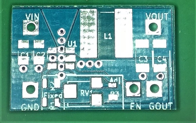
The copper, solder mask and drill accuracy were all very good and the vias were nicely tented.

Every board had a neatly routed outline, with no support tabs to remove, which is very nice.

The HASL surface isn’t as nice as ENIG, but it was perfectly adequate for my circuit.

The silkscreen registration was approximately half a mil too high and to the left on the top of the board. Also small text and graphics are noticeably pixelated. I’ve seen higher resolution silkscreen from other fabs.

An annoying feature is the tracking numbers that get added to every board (10220A-2/400958 above). Seeed decide where on your board to place this number.

Board Testing

I applied solder paste to a PCB with a stencil, populated the components, reflowed on a board heater and hand soldered the header pins.

Everything went smoothly and the circuit (a buck regulator) performed well at max current.


Making a buck converter

In my previous post I explained how to decide when you need a buck converter rather than a linear regulator. In this post I am going to explain how to build a buck converter into your project.

Drop in replacement

The simplest option, if you are used to using a linear regulator in a TO-220 package, is to buy a drop in replacement. For example Adafruit sell 1A 5V and 1A 3.3V drop in buck converters for just under $15 at the time of writing. Or for around $4.30 you could get a muRata OKI-78SR 1.5A 5V or 1.5A 3.3V module from DigiKey or Mouser.

From China

You can get small buck converters from China for a dollar or less, for an example search for Mini-360 buck converter. These are usually small PCBs with connection holes suitable for a wire or a header pin. The hole spacing is rarely breadboard compatible, but you can attach wires or carefully bend long header pins. They typically don’t come with datasheets, so you might want to test them before depending on the maximum advertised specifications. Shipping is slow, but you can’t beat the price.

Make your own

Finally you can make you own buck converter. Some reasons for building one yourself:

  • It is a great learning experience
  • You have complete control over and knowledge of the specifications
  • You can design the buck converter into the same PCB as the rest of your project

Picking components

There are thousands of buck converter ICs available. Your voltage and current requirements will help to narrow the field, but there will still be a large number to choose from. Other considerations are efficiency, frequency, circuit size, the number of external components, features, availability and price.

Small, simple and cheap

A common requirement is for a circuit that takes up a relatively small amount of board space at a reasonable cost. Unless you need a large amount of power a buck converter with built in MOSFETs will be ideal. While all in one modules do exist, they are currently much more expensive, so a few external components such as an inductor, capacitors and resistors are to be expected.

Efficiency, frequency and package

Improved efficiency means less heat is generated, requiring less space for thermal management, for this reason prefer synchronous designs that substitute a less efficient flyback diode for a second MOSFET. Higher frequency switching allows for smaller inductors and capacitors leading to a smaller design. Choose a package that matches you skills, avoid small packages like BGA unless you are used to working with them.

A handy search tool

Texas Instruments have a large number of buck converters, and nice tools for picking designs, you can try entering your criteria into the Power Quick Search tool.

And the winner is

My criteria for a recent project was a 12V input, 5V output and <500mA. I chose a Texas Instruments TPS560200 with the following specs:

  • 4.5V to 17V input
  • 0.8V to 6.5V output
  • 500mA maximum current
  • Synchronous
  • 80% efficiency
  • 600 KHz switching frequency
  • SOT-23 package
  • Light load efficiency, thermal protection and over current protection
  • Price about $0.89 for one, about $0.36 each for a real of 3000

This is a five pin SOT-23 surface mount component with about 0.04″/1mm lead pitch which should be manageable as a first surface mount design.

Picking passive components

A buck controller will generally need to be paired with the following components:

  • Input capacitor
  • Inductor
  • Output capacitor
  • Voltage divider resistors

The datasheet will provide guidance on how to pick the components. If you are using a TI buck controller then you can also use their WeBench tool to help you pick the right components for your design.

I don’t recommend the schematic and layout export from WeBench. My experience was that none of the wires were connected in the schematic and the board layout wouldn’t import into the free version of Eagle CAD.

Equivalent series resistance

In power circuits the capacitors are normally moving large amounts of current, so the equivalent series resistance, ESR, becomes an important consideration. For instance a typical 22uF electrolytic capacitor might have an ESR of 10 ohms whereas a multilayer ceramic capacitor might have an ESR of 10 mOhms (1/1000th).

In general:

  • Use ceramic multilayer XR5 or XR7 capacitors as they have very low equivalent series resistance. Otherwise look for low-ESR capacitors
  • You will generally pair a high frequency input bypass capacitor, usually 0.1uF, with a larger bulk capacitor, e.g. 10uF
  • You can use two capacitors in parallel to lower the ESR

Layout guidelines

There a several things to consider when laying out your circuit:

The current loop has high current slew rate so needs to be kept as small as possible to reduce parasitic inductance

    • Place the input bypass capacitor (small, high frequency) close to the IC
    • The input bulk capacitor should be reasonably close to the IC
    • Place the output capacitor close to the inductor
    • Connect directly to the ground plane

Removing heat

    • Use copper pours to improve heat dissipation
    • Use thermal vias to move heat to the bottom of the board

Watch out for noise from switching

    • Place the inductor close to the IC
    • Don’t expand copper to the inductor beyond what’s required for current
    • Keep the feedback return path away from the inductor and input capacitor

To improve efficiency

    • Don’t run ground plane under the inductor

Putting the rules into practice

Here is an example PCB layout for 5V 500mA Buck converter with breadboard friendly headers. U1 is a Texas Instruments TPS560200 buck controller IC. C1 and C2 are 10uF output capacitors. C3 is a 0.1uF input bypass capacitor and C4 is a 10uF input bulk capacitor. The R1 and R2 resistors act as a voltage divider on the feedback from the output to the IC. The ratio of the voltage divider determines the output voltage.

Buck Converter Layout

To minimize parasitic inductance in the current loop, the inductor and input capacitors are right next to the IC and the output capacitors are placed right next to the inductor. These current loop components are connected directly to a top layer ground pour which is connected to the bottom layer ground plane with lots of vias.

To maximize heat dissipation there are thermal vias underneath the IC and in the ground pour close to the IC to help move heat to the large ground plane on the bottom of the board. As this package doesn’t have a thermal pad around 40% of the heat will dissipate through the pins, so there are large pours connected to the ground pin and Vin pin.

To minimize switching noise the inductor is close to the IC and the connection to the IC hasn’t been expanded into a large copper pour. The traces and voltage divider resistors for the feedback signal have been routed away from the inductor.

Efficiency is optimized by adding a cutout in the ground plane under the inductor to avoid inductor efficiency being reduced by eddy currents forming in the ground plane.

Tented vias

Some of the thermal vias (smaller green circles) are very close to the SMD pads. This introduces some risk of an accidental connection to ground if the solder from the pads were to stray to the exposed copper of the via. To avoid this risk we can arrange for each via to be covered in solder mask, the term for this is a tented via.

OshPark PCB with Tented Vias

In the board above, ordered from OSH Park, you can see the 16mil tented vias. The annular rings of the small tented vias are covered in purple solder mask, whereas the annular rings for the large header pin vias are exposed.

Eagle CAD

To make small enough vias to fit under the package for your IC you may need to specify a new drill size if one of the default drill sizes isn’t appropriate. In Eagle CAD you can select a new 16mil drill size by selecting:

Change –> Drill –> … (New Drill)

Entering 0.016 (or 16mil) and then clicking on any existing vias you want to resize or using the “Draw a via” tool to create new vias.

The Eagle DRC (Design Rule Check) rules in Eagle typically specify that vias over a certain size should always have a stop mask. That is the copper annular ring should not be covered in solder mask.

Eagle Tented Via DRC

To ensure the thermal vias are tented (covered in solder mask) you should change the DRC rules so the stop mask is only automatically applied to vias larger than your selected tented via size, e.g. 16mil

Tools –> DRC –> Masks –> Limit –> 16mil

Then for vias 16mil or smaller you will be able to turn the stop mask on or off in the via properties.

KiCad

Creating thermal vias, also referred to as via stitching, can be confusing in the current version of KiCad as lone vias created by the Tracks And Vias tool will become disconnected from the GND net when you refill the filled zones or run DRC. There are plans to address this in version 5.0 of KiCad, but until then there are a couple of workarounds.

The simplest, if not the prettiest, is to make sure that your vias are connected to a GND pad with a track. The tracks will be absorbed by the copper pour (filled zone) so they don’t affect the final PBC.

The other solution is to create a new “via” footprint in Footprint Editor and add this footprint directly to your board in PcbNew.

To create a via footprint:

  • Launch Footprint Editor
  • Click New Component
  • Make the Name and Ref text Invisible
  • Add a pad at the origin (x=0, y=0)
  • Edit the pad
  • Set Copper to All Copper Layers
  • Remove F.Mask and B.Mask from Technical Layers to make the via tented
  • Set the hole size (e.g. 0.016″) and pad size (e.g. 0.03″)
  • Set Copper Zones Pad Connection to Solid
  • Save to an existing or new library with a name like via-16mil

To add the via footprint to you board

  • Click Add Footprint in Pcbnew
  • Click on the board and select your new via footprint (e.g. via-16mil)
  • Edit the pad (not the footprint)
  • Set the Net Name to GND

You can do this again to add another via or use Duplicate Footprint to copy an existing via footprint.

A finished example

Here is an example of a completed breadboard friendly 5V buck converter.

500ma DC-DC Buck Converter on a Breadboard

PCB populated and tested

Populated PCBI found some time last week to populate my OshPark board and test it. You can see it here connected to 12V power (bottom) and a 12V LED strip load (top).

Soldering the through the hole components didn’t take too long. I didn’t have any problem with the connections where I had omitted thermal relief, but they did take a little longer to heat up.


Thermal relief

If a component is connected directly to a large area of copper on a PCB such as a ground plane, the copper will conduct the heat away from the soldering iron making it more difficult to get everything hot enough to solder.

thermalreliefA thermal relief reduces this effect by adding short traces between the connection point and the copper area as shown in this illustration from Eagle.

I omitted the thermal relief on the 12V power connections to ensure the traces could carry plenty of current without heating up.

Having large traces and direct ground plane connections for the high current part of the circuit is necessary as thin traces will heat up if too much current is passed through them, wider traces can carry more current.

My LED strip is only drawing 1.25A, so this might be overkill as I only need 16.5 mil of trace to carry a 1.25A load with a 10 degrees centigrade temperature rise. But it seemed like a good idea to design in some extra current carrying capacity.

The MOSFET I used can switch 16A, but in its TO-220 package it already has a thermal rise of 6.84 degrees centigrade at 1.25A without a heat sink. So I would probably want to add a heat sink to switch more than 3A.

Programming

I tuned the adjustable DC/DC buck converter (green daughter board) to supply the board with a 5V and everything looked good electrically. So I inserted the XBee and the ATTiny85 microcontroller.

I attached a SparkFun ATTiny programmer to the board using a 6 pin ISP cable and uploaded my software to the ATTiny85.

The buttons worked as expected, but I was disappointed to discover that the IR and XBee serial input were not working correctly.

Debugging

The SparkFun ATTiny programmer is a great $20 programmer, but it doesn’t provide any debugging functionality so I resorted to the age old technique of modifying the code and flashing an LED to indicate what was going on.

I took the time to fix a bug, which I already knew about, that would cause the IR input to malfunction if a serial input occurred at the same time, but things were still not working correctly. When using interrupts you have to think carefully about what would happen if an interrupt triggered at an inopportune moment.

Then I noticed that the serial input was low when it should have be high. The XBee serial out should always be high unless it is sending data to the ATTiny85. When I checked the XBee serial output was indeed high, but the signal wasn’t triggering a high on the ATTiny digital input.

In Circuit Programmers

An ATTiny85 only has eight pins, for power, programming, and input/output. Programming the ATTiny requires six pins: GND, 5V, Reset, SCK, MOSI and MISO. My circuit requires 7 pins: GND, 5V, Up Button, Down Button, Serial input, IR input, PWM output. To accommodate these eleven different functions on 8 pins requires that the programming and I/O functions share the same pins.

For the programmer to work effectively while the ATTiny is in-circuit it is important that the circuit doesn’t interfere with the programmer. For things like buttons, this isn’t a huge problem – use large value pull-up resistors and don’t press a button in the middle of programming, but for the serial input pin this is a problem as the line is being held high even when there is no serial activity.

So I put a 1K resistor between the XBee serial output and the ATTiny85 serial input so it would not interfere with use of the pin as MOSI during programming. The XBee voltage is only 3.3V, but the trigger voltage of the ATTiny85 is 2.5V (with 5V power) so it can still trigger a high digital input. Adding the resistor directly between the XBee serial output and the ATTiny85 input doesn’t cause any noticeable voltage drop, so this approach works well.

Blinking LEDs

However, the SparkFun ATTiny programmer has a yellow LED connected to this same pin via a 330 ohm resistor. This is nice as you have an LED you can blink for testing and debugging on pin 0. Pin 0 can be a digital output in addition to a serial input and MOSI.

However this feature of the programmer caused the voltage to the ATTiny serial input to be dropped too low as the 330 ohm resistor and the 1K resistor act as a voltage divider with the ATTiny serial input pin in the middle.

Voltage Divider Calculation With An LED

The addition of the LED makes the voltage divider calculation a little more interesting. The voltage divider needs to be applied to the voltage between 3.3V and the LED, which means we must subtract the voltage drop of the LED first.

The yellow LED will drop the voltage by its forward voltage. Yellow LEDs are quoted as having a forward voltage of 2.1V, but that is at their brightest – it is a useful value to calculate the value of a resistor that will not cause the LED to burn out. However, with the 1K and 330 ohm resistors between the LED and 3.3V the LED is only drawing 1 to 2 mA of current and will only drop the voltage by about 1.7V. The datasheet show a graph of forward voltage by current.

So the voltage divider needs to be applied to 3.3V – 1.7V = 1.6V. The voltage divider equation is Vout = Vin*R2/(R2+R1). Where R2 is 330 ohms and R1 is 1K. See Wikipedia for details.

Vout = 1.6 * 330/(1000+330) = 0.4 V

Then we just add back the forward voltage of the LED to get the full voltage for that point in the circuit.

1.7 + 0.4 = 2.1 V

Which is below the 2.5V trigger threshold of the ATTiny85. So the ATTiny85 reads this as a digital low.

The Fix

As far as my code was concerned the serial input was continuously setting a zero dimming level. The simple fix was to unplug the programmer, upon which everything started working perfectly!

A workaround for testing the circuit with the programmer attached is to use a strong enough pull up resistor to push the serial input over 2.5V. I chose to add a 1K pull up resister between MOSI and 5V on the programmer which will add 0.6V. This is a similar voltage divider to above, but with a 5V input rather than a 3.3V input. I attached this to the header pins on the programmer, but I don’t want to make this a permanent addition to my PCB as 1K is rather a strong pull up which would draw unnecessary quiescent current when the programmer isn’t attached.


The next step is to design and 3D print an enclosure.


My First PCB

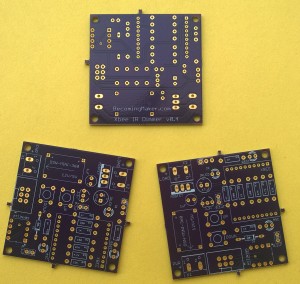
Circuit BoardsI have received my first printed circuit boards from OSH Park. They look great and I am looking forward to trying them out.

I have designed my own circuits, prototyped them on breadboards and soldered them onto protoboard before, but I really wanted to take the next step and produce a real PCB.

12V LED Dimmer

The PCB circuit is a dimmer control for a 12V LED lighting strip. It provides three means of control:

  1. Buttons on the device
  2. An IR remote control
  3. XBee from a computer

I thought I would make my first boards using through the hole components, but I would like to try surface mount next.

OSH Park ordering experience

These are double sided 2″ by 2″ boards and three boards cost me $19.95 including shipping. OSH Park charge $5 per square inch for three and you can order as many boards as you like, as long as they are in multiples of three.

I ordered the boards and received an email the same day indicating that they were awaiting panelization. OSH Park takes small orders, from Makers like you and me, and groups them together to fill an 18″ x 24″ PCB fabrication panel. When they fill up a panel they send the design file off to the fabricator to be manufactured.

Two days later I received another email telling me that the panel had been sent to the manufacture and they expected to get it back in four days. They even mentioned that there were 36 other orders on the panel and a total of 294 boards.

Three days later they told me that the panel had arrived back from the fabricator and that they expected them to be depanelled and shipped within 48 hours. The panel contains lots of boards connected together by little tabs with three small holes on each side. This enables the individual boards to be broken off the panel. If you look at the picture of my boards you can see some of the tags still attached.

Seven minutes later I received an email telling me that my boards had been shipped. That email included a USPS tracking number.

Two days later a padded envelope containing the boards arrived at my house. So it took seven days from the date that I ordered the boards for them to arrive.

I think that’s pretty awesome price ($19.95) and turnaround time (7 days) for three custom PCBs. As a comparison if I ordered three 2″ x 2″ protoboards from SparkFun they would cost me $15.71 including economy shipping. And it’s nice getting frequent updates on where your board is in the process.

I have shared the board here on OSH Park.

Designing a board

I designed the board using an application called Eagle. CadSoft the company that make Eagle are generous enough to make a freeware version available which is very popular with Makers. You can download it from:

http://www.cadsoftusa.com/download-eagle/

The free version limits your schematic to a single sheet and your board size to 4″ x 3.2″, but that is more than good enough for most Makers.

Eagle takes a bit of getting used to as it is mode based: click to add a component and you’re stuck adding components to your board until you select a different mode from the toolbox on the left. But it’s worth investing in learning it as it opens up a whole new world of possibilities.

There are other circuit board design applications out there, but Eagle is one of the most popular. Also OSH Park will allow you to upload your Eagle files directly, which is nice for a first timer as it cuts out the step of generating Gerber files.

So now I need to find the time to solder some components to the board, with nearly one hundred holes on this board, it might take me a while!